Sunday, July 2, 2023

The VL53L8 8x8 laser ranging sensor

The sensor

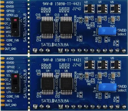
A VL53L8 is a continuation of a family of laser ranging sensors from ST. They use Single Photon Avalanche Diodes in an 8x8 array giving a pyramid of distances projected out from the sensor from ranges of 2-400cms. It can also do 4x4 with SW interpolation.

I ordered a sensor (set) from ST. 

511-SATEL-VL53L8

You get two sensors on breakout boards for your $27. This is good because w/o this fancy breakout board, you will be on the hook for generating 1.2 & 1.8v.


Wired up to a modified Bluepill with an STM32L443 as a donor CPU, via some simple Dupont wiring, we can communicate with the sensor via I2C. SPI is also possible but the example code that ST provides that was used to debug the comm was I2C and this made comparing easier.

Ada driver

An Ada driver was crafted for the sensor. This was a translation of ST's API for the VL53L8. It was a job to translate it. There is 90k of FW that needs to get DL'd into the sensor. Numerous blind writes to undocumented proprietary registers. But... the important parts are there. If you follow the sequence and do as they do, the device can be brought up w/o error. Hindsight, perhaps using a hybrid project of C/Ada might work but the data structures between the C impl and the Ada might be a snag. Maybe a wrapper could work though. In the end there is an Ada driver for it but at what cost and what did Ada really bring to the table? If the sensor bringup is just a bunch of blind writes, C is perfectly fine for that. Still, the work is done. We have an Ada driver, lets use it. 

Ada stacksize

I ran into an interesting issue with the sensors FWDL. In Ada's I2C implementation, if you want to write to a 16 bit register on a device it looks as so:

<i2c addr><hi_index><lo_index><data .....>

How Adacores's top level I2C implementation handled that was as so:


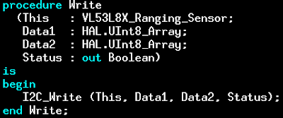
Observe, this makes a new array composed of the indices and the data. This is fine for small data writes, which is the norm for most device I2C transactions. The VL53L8 though with its 90+K of FW is a challenge here. ST sends the FW in 32K chunks, so at a minimum, 32K will now go on the stack to produce the new buffer. The solution I came up with was a two array write.


Of course there is a commensurate I2C_Write and Master_Transmit that accept two arrays. The win here is no extra stack usage and my STM32L443 is now using a reasonable stack. During debug, I had less than 32 bytes free I think (all of the 64K was consumed due to the giant stack).

The caller in the driver can then say:


Prev, the index was passed in in this case as 16#0000#.

There are some other cases that are large DL's also. crosstalk, default_config. Those also use the scheme.


I think 16#7fff# is some form of bank select for the part. I wonder if the index of 0 is the offset into that bank. If so, perhaps the FWDL could have been done using the existing Ada code and just send less each time.

Ranging

That's what were here for. What happens when you issue a ranging command.


So what is in results?


Looking at distance_mm ranging on a white cube that is both angled and tipped

angled l->r (l closer to pin1 arrow)
+ tipped (top further from pin1)
0x40, 0x42, 0x3c, 0x3b, 0x36, 0x38, 0x32, 0x2f,        greater right
0x3e, 0x3b, 0x35, 0x33, 0x33, 0x32, 0x2d, 0x2d,
0x3b, 0x39, 0x35, 0x30, 0x2f, 0x2e, 0x2e, 0x2a, | gt top -> less |
0x39, 0x33, 0x31, 0x2e, 0x2b, 0x28, 0x27, 0x28,
0x35, 0x2f, 0x2f, 0x2d, 0x27, 0x27, 0x26, 0x26,
0x2f, 0x2e, 0x28, 0x2a, 0x27, 0x24, 0x24, 0x23,
0x2d, 0x2b, 0x2a, 0x28, 0x24, 0x23, 0x22, 0x23,
0x29, 0x26, 0x25, 0x22, 0x22, 0x22, 0x21, 0x21          less left

Thus (0) is furthest and (63) closest

The accuracy gel's with ST's data that its +/- 2mm. I found that to be quite accurate over the measured area.

So if you rotated that 2D matrix 90 degrees clockwise it would look like what I see from the physical setup.

Code

https://github.com/morbos/STM32/blob/master/L/L443/vl53l8x_l443/src

Sunday, December 18, 2022

The Air32F103

 Bluepills

Its no surprise that Bluepills, such as they were, a smoking sub $2 deal would dry up eventually, taken over by clones, some subtle, some overt. With supply issues still plaguing ST parts for hobbyists, what about these cheap Chinese clone parts? Lets dive into the Air32F103.

Air32F103

I bought 5 of these $1.90 boards. They look like this:


Some notables vs a stock bluepill:

1) Castellated pins with flat underside for use as a module

2) 3 LEDs R/G/B (vs just the G for a bluepill)

3) Clone of ST's peripherals

4) over clockable to 256Mhz (spec is 216Mhz) (original STM32F103CB is 72Mhz)

5) 32K of ram. But, via secret regs, 97K(!)

6) top and bottom debug pads, top for JLINK, bottom, legacy STLINK SWD

7) USB C vs USB mini

8) BOOT as a button vs jumper

9) 2 12bit DACs (STM32F103CB's don't have that)

10) QSPI (hidden support)

11) Undocumented crypto block from MegaHunt (includes: AES/DES/3DES/SHA/SM[1,3,4,7])

Clocking

As mentioned 256Mhz is possible. One Q is how do they do that? Well, PLLMUL is a 4bit field so 8Mhz * 16 gets a max of 128Mhz. A new bit, bit28 of RCC.CFGR adds 16 to the MUL. So, 31(+1) gets 256Mhz.

So, if you do set that, the code will crash with a usage fault. There is secret code called in the ROM that flips a hidden bit to allow high speed operation (the SysFreq_Set code below)

The RCC init code from:

https://gitee.com/openLuat/luatos-soc-air32f103/

https://gitee.com/openLuat/luatos-soc-air32f103/blob/master/Libraries/AIR32F10xLib/src/air32f10x_rcc_ex.c

Here we see the 97K unlock:

Observe they flip the lock at the end and revert back to 32K sram

In my Ada code, I flip the lock but seem to fail to revert it back.. leaving 97K available.

The magic reg to allow for high speed op is as follows:

     Magic_Reg : UInt32 with Volatile, Address => System'To_Address (16#40022214#);
...
         --  Hidden system reg block --
         --  w/o this.. 216Mhz progs don't run (usage fault) --
         Magic_Reg := Magic_Reg or 1;

Conclusions
I really don't think you can misstep here, $1.90 (aliexpress price) for a board with all those features.
There are some differences that need exploration:
https://wiki.luatos.com/chips/air32f103/switchFromSxx.html#air32f103

Have fun! To quote Hunz on value for money wrt hacking:
https://youtu.be/7kNeaj36VbE?t=2963

Disassembly backup material for the rom study
On entry
r0             0x10280000          271056896
r1             0x1                 1
r2             0x0                 0
r3             0x1
0x1fffe97c: push {r4, r5, r6, lr}
   0x1fffe97e: mov r6, r1
   0x1fffe980: mov r1, r0
   0x1fffe982: sub sp, #24
   0x1fffe984: mov r4, r3
   0x1fffe986: mov r5, r2
   0x1fffe988: movs r0, #0
   0x1fffe98a: bl 0x1fffe12c
; read 0x40021004 (reads 0)
        0x1fffe12c: ldr r3, [pc, #12] ; (0x1fffe13c)
        0x1fffe12e: ldr r2, [r3, #4]
; or in the PLLMUL
        0x1fffe130: orrs r0, r1
; clear PLLMUL field
        0x1fffe132: bic.w r2, r2, #4128768 ; 0x3f0000
; or in prior contents(why?)
        0x1fffe136: orrs r0, r2
; final PLLMUL (0x10280000) (thats +16 and 10 mult (27 * 8 = 216)
        0x1fffe138: str r0, [r3, #4]
        0x1fffe13a: bx lr
   0x1fffe98e: movs r0, #0
   0x1fffe990: bl 0x1fffe0d8
   ; read 0x40021004
        0x1fffe0d8: ldr r2, [pc, #12] ; (0x1fffe0e8)
; reads old val 0x10280000
        0x1fffe0da: ldr r1, [r2, #4]
; wipe HPRE
        0x1fffe0dc: bic.w r1, r1, #240 ; 0xf0
; or in wanted val (in this case 0)
        0x1fffe0e0: orrs r1, r0
; no change to HPRE
        0x1fffe0e2: str r1, [r2, #4]
        0x1fffe0e4: bx lr
   0x1fffe994: mov.w r0, #1024 ; 0x400
   0x1fffe998: bl 0x1fffe0f8
        0x1fffe0f8: ldr r2, [pc, #12] ; (0x1fffe108)
        0x1fffe0fa: ldr r1, [r2, #4]
; Now PPRE1 (set to the 0x4 of r0's arg of 0x400)
        0x1fffe0fc: bic.w r1, r1, #1792 ; 0x700
        0x1fffe100: orrs r1, r0
        0x1fffe102: str r1, [r2, #4]
;(gdb) x/x 0x40021004
;0x40021004: 0x10280400
        0x1fffe104: bx lr
   0x1fffe99c: movs r0, #0
   0x1fffe99e: bl 0x1fffe10c
; we arrive with r0=0
        0x1fffe10c: ldr r2, [pc, #12] ; (0x1fffe11c)
        0x1fffe10e: ldr r1, [r2, #4]
; once again 0x40021004
; PPRE2
        0x1fffe110: bic.w r1, r1, #14336 ; 0x3800
        0x1fffe114: orr.w r0, r1, r0, lsl #3
        0x1fffe118: str r0, [r2, #4]
; 0x10280400
        0x1fffe11a: bx lr
   0x1fffe9a2: mov r0, sp
;(gdb) x/16x $r0
;0x20000fd8: 0x00000000 0x00000000 0x00000000 0x00000000
;0x20000fe8: 0x00000000 0x00000000 0x00010000 0x10280000
;0x20000ff8: 0x00000001 0x0800136d 0x200183ff 0x08001464
;0x20001008: 0x08001464 0x00000000 0x00000000 0x080002dd
   0x1fffe9a4: bl 0x1fffe004
        0x1fffe004: push {r4, r5, lr}
        0x1fffe006: ldr r2, [pc, #144] ; (0x1fffe098)
        0x1fffe008: ldr r1, [r2, #4]
; once again 0x40021004 = 0x40021004
        0x1fffe00a: ldr r3, [pc, #144] ; (0x1fffe09c)
; r3=0x7a1200
; SWS masked off (0xC)
        0x1fffe00c: ands.w r1, r1, #12
; vvv taken since after masking, r1 == 0
        0x1fffe010: beq.n 0x1fffe01a
        0x1fffe012: cmp r1, #4
        0x1fffe014: beq.n 0x1fffe01a
        0x1fffe016: cmp r1, #8
        0x1fffe018: beq.n 0x1fffe01e
; Save r3 on the stack
        0x1fffe01a: str r3, [r0, #0]
;(gdb) x/x $r0
;0x20000fd8: 0x007a1200
        0x1fffe01c: b.n 0x1fffe054
        0x1fffe01e: ldr r1, [r2, #4]
        0x1fffe020: ldr r3, [r2, #4]
        0x1fffe022: and.w r1, r1, #3932160 ; 0x3c0000
        0x1fffe026: ldr r4, [r2, #4]
        0x1fffe028: and.w r3, r3, #65536 ; 0x10000
        0x1fffe02c: lsrs r4, r4, #27
        0x1fffe02e: lsls r4, r4, #31
        0x1fffe030: beq.n 0x1fffe03c
        0x1fffe032: movs r4, #16
        0x1fffe034: orr.w r1, r4, r1, lsr #18
        0x1fffe038: adds r1, r1, #1
        0x1fffe03a: b.n 0x1fffe042
        0x1fffe03c: movs r4, #2
        0x1fffe03e: add.w r1, r4, r1, lsr #18
        0x1fffe042: cbz r3, 0x1fffe04a
        0x1fffe044: ldr r3, [r2, #4]
        0x1fffe046: lsls r3, r3, #14
        0x1fffe048: bpl.n 0x1fffe04e
        0x1fffe04a: ldr r3, [pc, #84] ; (0x1fffe0a0)
        0x1fffe04c: b.n 0x1fffe050
        0x1fffe04e: ldr r3, [pc, #76] ; (0x1fffe09c)
        0x1fffe050: muls r1, r3
        0x1fffe052: str r1, [r0, #0]
; ^^^ from 0x1c above
; ld 0x40021004 again...
        0x1fffe054: ldr r1, [r2, #4]
        0x1fffe056: movs r3, #15
;??? why
        0x1fffe058: and.w r1, r3, r1, lsr #4
; HPRE now in r1 (r1 >> 4) & 0xF
        0x1fffe05c: ldr r3, [pc, #68] ; (0x1fffe0a4)
; r3=0x20018050 (the secret memory)
; some sort of byte table indexed by r1
        0x1fffe05e: ldrb r4, [r3, r1]
; reads 0
        0x1fffe060: ldr r1, [r0, #0]
; read back tos (0x7a1200)
; this is a shift by 0 (r4 == 0)
        0x1fffe062: lsrs r1, r4
; write back tos+4 same 0 shifted# 0x7a1200
        0x1fffe064: str r1, [r0, #4]
; read 0x40021004 again...
        0x1fffe066: ldr r4, [r2, #4]
        0x1fffe068: movs r5, #7
; get 10:8 into r4 (was 0x400 -> PPRE1=4)
        0x1fffe06a: and.w r4, r5, r4, lsr #8
; this reads 0x20018054[7:0] = 1
        0x1fffe06e: ldrb r4, [r3, r4]
; now shift 7a1200 by... r4(==1)
        0x1fffe070: lsr.w r4, r1, r4
; r4 0x3d0900
; 0x20000fd8: 0x007a1200 0x007a1200 0x003d0900 0x00000000
        0x1fffe074: str r4, [r0, #8]
; still 0x40021004 == 0x10280400
        0x1fffe076: ldr r4, [r2, #4]
; read PPRE2
        0x1fffe078: and.w r4, r5, r4, lsr #11
; r4=0, read is 0
        0x1fffe07c: ldrb r3, [r3, r4]
; r1=0x7a1200 << 0, unchanged
        0x1fffe07e: lsrs r1, r3
; after this str
; (gdb) x/8 $r0
; 0x20000fd8: 0x007a1200 0x007a1200 0x003d0900 0x007a1200
        0x1fffe080: str r1, [r0, #12]
; CFGR again...
        0x1fffe082: ldr r2, [r2, #4]
; ADCPRE
        0x1fffe084: movs r3, #3
; ADCPRE was 0
        0x1fffe086: and.w r2, r3, r2, lsr #14
        0x1fffe08a: ldr r3, [pc, #24] ; (0x1fffe0a4)
; backup magic ram to 0x2001804c...btw 0x4c = 0x08060402
        0x1fffe08c: subs r3, r3, #4
; r2=0 this should read 2
        0x1fffe08e: ldrb r2, [r3, r2]
; r2=2 div 8mhz by 2
        0x1fffe090: udiv r1, r1, r2
; r1 == 4mhz (0x3d0900)
        0x1fffe094: str r1, [r0, #16]
0x20000fd8: 0x007a1200 0x007a1200 0x003d0900 0x007a1200
0x20000fe8: 0x003d0900 0x00000000 0x00010000 0x10280000
        0x1fffe096: pop {r4, r5, pc}
; 0x40022000 secret peripheral
   0x1fffe9a8: ldr r0, [pc, #40] ; (0x1fffe9d4)
; read 0x40022214 (== 0x00034069)
   0x1fffe9aa: ldr.w r1, [r0, #532] ; 0x214
   0x1fffe9ae: movw r2, #49159 ; 0xc007
; r1 now becomes 0x30068
   0x1fffe9b2: bics r1, r2
; r6 (==1) arg save from entry
   0x1fffe9b4: and.w r2, r6, #7
; r2 is now 1
; which makes r1=0x30069
   0x1fffe9b8: orrs r1, r2
; r4 was 1 so this is 1
   0x1fffe9ba: and.w r2, r4, #1
; r1=0x30069
   0x1fffe9be: orr.w r1, r1, r2, lsl #14
; now 0x34069  r2=0 after the and
   0x1fffe9c2: and.w r2, r5, #1
; making r1 unchanged (0x34069)
   0x1fffe9c6: orr.w r1, r1, r2, lsl #15
   0x1fffe9ca: str.w r1, [r0, #532] ; 0x214
   0x1fffe9ce: add sp, #24
   0x1fffe9d0: pop {r4, r5, r6, pc}


Sunday, October 30, 2022

 The GD32VF103

This chip is a peripheral clone of an STM32F103. The CPU is swapped out for a Risc-V.


Openocd debug using JTAG

Using the release on github:
https://github.com/riscv/riscv-openocd
Build it:
./bootstrap 
./configure --enable-ftdi --enable-stlink --enable-ti-icdi --enable-jlink --enable-cmsis-dap --enable-xds110
make
 
We can connect to the target.

Wiring to a J-Link is as so:

ARM20 JTAG:
Pin1 VCC -> 3V3
Pin3 TRST -> RESET
Pin5 TDI -> JTDI (underside of board)
Pin7 TMS -> JTMS
Pin9 TCLK -> JTCLK
Pin13 TDO -> JTDO

Add this to openocd/tcl/board as bluepillGDF103.cfg

adapter speed 8000
source [find interface/jlink.cfg]
source [find target/longan.cfg]
jtag_ntrst_assert_width 10
reset_config trst_only

Add this to openocd/tcl/target as longan.cfg:

# script for Longan nano

#
# longan nano devices support JTAG
#
transport select jtag

if { [info exists CHIPNAME] } {
   set _CHIPNAME $CHIPNAME
} else {
   set _CHIPNAME riscv
}

set _ENDIAN little

if { [info exists DAP_TAPID] } {
set _DAP_TAPID $DAP_TAPID
} else {
        set _DAP_TAPID 0x1000563D
}

jtag newtap $_CHIPNAME cpu -irlen 5 -expected-id $_DAP_TAPID
set _TARGETNAME $_CHIPNAME.cpu
target create $_TARGETNAME riscv -chain-position $_TARGETNAME
$_TARGETNAME configure -work-area-phys 0x20000000 -work-area-size 20480 -work-area-backup 0

# Work-area is a space in RAM used for flash programming
if { [info exists WORKAREASIZE] } {
   set _WORKAREASIZE $WORKAREASIZE
} else {
   set _WORKAREASIZE 0x5000
}

# Allow overriding the Flash bank size
if { [info exists FLASH_SIZE] } {
    set _FLASH_SIZE $FLASH_SIZE
} else {
    # autodetect size
    set _FLASH_SIZE 0
}

# flash size will be probed
set _FLASHNAME $_CHIPNAME.flash

#flash bank $_FLASHNAME gd32vf103 0x08000000 0 0 0 $_TARGETNAME
flash bank $_FLASHNAME stm32f1x 0x08000000 0 0 0 $_TARGETNAME
riscv set_reset_timeout_sec 1
init

halt


Run openocd:
root@ubuntu:/p4work/riscv-openocd/tcl# ../src/openocd -f board/bluepillGDF103.cfg
Open On-Chip Debugger 0.11.0+dev-02415-gfad123a (2022-10-29-17:33)
Licensed under GNU GPL v2
For bug reports, read
http://openocd.org/doc/doxygen/bugs.html
Info : J-Link ARM V8 compiled Dec  1 2009 11:42:48
Info : Hardware version: 8.00
Info : VTarget = 3.339 V
Info : clock speed 8000 kHz
Info : JTAG tap: riscv.cpu tap/device found: 0x1000563d (mfg: 0x31e (Andes Technology Corporation), part: 0x0005, ver: 0x1)
Info : JTAG tap: auto0.tap tap/device found: 0x790007a3 (mfg: 0x3d1 (GigaDevice Semiconductor (Beijing) Inc), part: 0x9000, ver: 0x7)
Warn : AUTO auto0.tap - use "jtag newtap auto0 tap -irlen 5 -expected-id 0x790007a3"
Info : [riscv.cpu] datacount=4 progbufsize=2
Error: [riscv.cpu] Hart doesn't exist.
Error: [riscv.cpu] Hart is not halted!
Info : [riscv.cpu] Examined RISC-V core; found -1 harts
Info : [riscv.cpu]  XLEN=32, misa=0x40901105
[riscv.cpu] Target successfully examined.
Info : starting gdb server for riscv.cpu on 3333
Info : Listening on port 3333 for gdb connections
trst_only separate trst_push_pull

Info : Listening on port 6666 for tcl connections
Info : Listening on port 4444 for telnet connections

Not sure what the Hart not existing messages are about. Hardware Thread is my understanding of what a Hart is. No matter, GDB can attach, and reset the target. Note that the Risc-V came from Andes Technology. This is a TW IP provider, GigaDevice semi just does the integration with 'their' peripherals. Curious how they copied ST's peripherals, there is a lot in those peripherals so it would be a real job to make a workalike.

Flash programmed from openocd

Seems to work:

(gdb) load
Loading section .text, size 0x12b4 lma 0x50000
Loading section .rodata, size 0x1bc lma 0x512b4
Loading section .eh_frame, size 0x3c lma 0x51470
Loading section .sdata, size 0x3b lma 0x514ac
Start address 0x00050000, load size 5351
Transfer rate: 6 KB/sec, 1337 bytes/write.
(gdb) x/32x 0
0x0: 0xfffb1197 0x80018193 0xfffb1117 0xa5810113
0x10: 0x00001517 0x49c50513 0xfffb0597 0xfe858593
0x20: 0xfffb0617 0x01b60613 0x00c5fa63 0x00052283
0x30: 0x0055a023 0x05910511 0xfec5eae3 0xfffb0517

UART

Good old UART works. Hold reset then hold boot0 release in same order.
Connect a USB to UART adapter to the board. VCC -> 5V pin, GND to GND, Green wire to R0, White to T0. (at least those are the colours on my Adafruit adapter).

Ubuntu can install stm32flash. Then, a raw binary (the -f flag) programs the FW. Watch out with /dev/ttyUSB0, by default its root owned so stm32flash may fail.

stm32flash -g 0x08000000 -b 115200 -w firmware.bin -f /dev/ttyUSB0

Software

Using Fabien Chouteau's PicoRV32 example code. Its Ada Zero Footprint. Linked at 0. 


Monday, May 25, 2020

SVD file optimization


Optimizing SVD files

SVD files, what are they?


This webpage has a good overview, after all, they penned the format:

https://www.keil.com/pack/doc/CMSIS/SVD/html/index.html

Basically, its an XML file that describes an SoC from peripherals to registers to individual fields. Typically sucked in by a debugger to get a meaningful view into an SoC. Its also been used as an input to some very useful tools, such as...

svd2ada

When I started looking at Ada for embedded ARM hacking some years back. Adacore had an early library, Ada_Drivers_Library. It had drivers for all the peripherals in some STM32F4 series parts. How it did this was interesting, underneath the driver was a description of the HW from a bunch of .ads files that were... automatically generated. Adacore had written a tool. svd2ada, that would parse the SVD file provided by the vendor, in this case ST microelectronics, and produce a detailed specification of each peripheral in the part along with type records for each register and enclosed fields. Quite eye opening to me. Having waded through many vendors C .h files that were festooned with #define masks all over the place to describe in a flat, non-hierarchical fashion the encoding of fields in regs.

Example

Here is a peripheral from the STM32L562, the on-the-fly decryption engine. We see the name of the peripheral, a description and the all important base address:

<peripheral>
      <name>OTFDEC1</name>
      <description>On-The-Fly Decryption engine</description>
      <groupName>OTFDEC</groupName>
      <baseAddress>0x420C5000</baseAddress>

Lets look at a register from this peripheral:
        <register>
          <name>R1CFGR</name>
          <displayName>R1CFGR</displayName>
          <description>OTFDEC region x configuration
          register</description>
          <addressOffset>0x20</addressOffset>
          <size>0x20</size>

and another:
        <register>
          <name>R2CFGR</name>
          <displayName>R2CFGR</displayName>
          <description>OTFDEC region x configuration
          register</description>
          <addressOffset>0x50</addressOffset>
          <size>0x20</size>

See a pattern? Each register is a name with a number embedded and its offset is rising by a value > the size in bits... we will look at that observation later.

Now traditionally, svd2ada would process this as you see it in the XML and the stm32_svd-otfdec.ads would look like this:

      R1CFGR      at 16#20# range 0 .. 31;
      R1STARTADDR at 16#24# range 0 .. 31;
      R1ENDADDR   at 16#28# range 0 .. 31;
      R1NONCER0   at 16#2C# range 0 .. 31;
      R1NONCER1   at 16#30# range 0 .. 31;
      R1KEYR0     at 16#34# range 0 .. 31;
      R1KEYR1     at 16#38# range 0 .. 31;
      R1KEYR2     at 16#3C# range 0 .. 31;
      R1KEYR3     at 16#40# range 0 .. 31;

...
      R4CFGR      at 16#B0# range 0 .. 31;
      R4STARTADDR at 16#B4# range 0 .. 31;
      R4ENDADDR   at 16#B8# range 0 .. 31;
      R4NONCER0   at 16#BC# range 0 .. 31;
      R4NONCER1   at 16#C0# range 0 .. 31;
      R4KEYR0     at 16#C4# range 0 .. 31;
      R4KEYR1     at 16#C8# range 0 .. 31;
      R4KEYR2     at 16#CC# range 0 .. 31;
      R4KEYR3     at 16#D0# range 0 .. 31;

Now, there is a lot of commonality in those reg groups I think we can see. So the question becomes is there a more compact way to describe the layout of these repetitive groupings?

Well, it turns out, there is. SVD files have some other nomenclature that permits descriptions of this type of repetitive grouping. The term SVD uses is cluster and dim (or <cluster> and <dim> in XML). These terms allow specification of such groups in a form that is indexable by software. Fortunately for us, svd2ada already supports <cluster> and <dim>. Super news for us, if only there was a way to automatically emit these compressive constructs so we don't have to sift through 500k XML files performing hand edits.

3) svdopt.rb
If there was a tool that could parse the SVD file, identify those groupings and re-write the SVD file with those changes, then the indexable records ought to have a more compact form that should reduce the amount of code needed in an Ada driver to work with the peripheral. Taking the example above, if left unchanged, you would have code to handle R1CFGR... R2... R3.. R4 where, realistically, RxCFGR would do if you had an array of records. So a tool was crafted. It accepts an SVD file as input and produces an SVD file as output. It tries to be automatic in processing but we will get to special cases later. For now lets look at the definition for R1CFGR which we saw above. This cluster below describes all the regs in the group. Observe, R is taken as the cluster name as all the RxY use R as the lead-in to the element. The <cluster> has a dim of 4 which matches the HW desc. There is a new field I added <dimOffset> that shows 1. Given SVD files are C oriented, they assume arrays begin at 0. Well Ada doesn't have to do that, and neither does the reference manual and vendor SVD. They start this register group a 1 so... we have a syntax to allow that also. Observe also that this <cluster> has an array embedded inside each element. the RxKEYy and RxNONCEy values. So the tool correctly identifies this from the description and emits embedded <dim> accordingly.

<cluster>
  <dim>4</dim>
  <dimIncrement>0x30</dimIncrement>
  <dimOffset>1</dimOffset>
  <name>R[%s]</name>
  <addressOffset>0x20</addressOffset>
  <register>
    <name>CFGR</name>
    <displayName>CFGR</displayName>
    <description>OTFDEC region x configuration register</description>
    <addressOffset>0x0</addressOffset>
    <size>0x20</size>
    <access>read-write</access>
    <resetValue>0x00000000</resetValue>
    <fields>
      ...
    </fields>
  </register>
  <register>
    <name>STARTADDR</name>
    <displayName>STARTADDR</displayName>
    <description>OTFDEC region x start address register</description>
    <addressOffset>0x4</addressOffset>
    <size>0x20</size>
    <access>read-write</access>
    <resetValue>0x00000000</resetValue>
    <fields>
    </fields>
  </register>
  <register>
    <name>ENDADDR</name>
    <displayName>ENDADDR</displayName>
    <description>OTFDEC region x end address register</description>
    <addressOffset>0x8</addressOffset>
    <size>0x20</size>
    <access>read-write</access>
    <resetValue>0x00000000</resetValue>
    <fields>
      <field>
        <name>REGx_END_ADDR</name>
        <description>Region AXI end address</description>
        <bitOffset>0</bitOffset>
        <bitWidth>32</bitWidth>
      </field>
    </fields>
  </register>
  <register>
    <dim>2</dim>
    <dimIncrement>4</dimIncrement>
    <dimOffset>0</dimOffset>
    <name>NONCER[%s]</name>
    <addressOffset>0xc</addressOffset>
    <size>0x20</size>
    <access>read-write</access>
    <resetValue>0x00000000</resetValue>
    <fields>
      <field>
        <name>REGx_NONCE</name>
        <description>REGx_NONCE</description>
        <bitOffset>0</bitOffset>
        <bitWidth>32</bitWidth>
      </field>
    </fields>
  </register>
  <register>
    <dim>4</dim>
    <dimIncrement>4</dimIncrement>
    <dimOffset>0</dimOffset>
    <name>KEYR[%s]</name>
    <addressOffset>0x14</addressOffset>
    <size>0x20</size>
    <access>read-write</access>
    <resetValue>0x00000000</resetValue>
    <fields>
      <field>
        <name>REGx_KEY</name>
        <description>REGx_KEY</description>
        <bitOffset>0</bitOffset>
        <bitWidth>32</bitWidth>
      </field>
    </fields>
  </register>
</cluster>

svd2ada result

Well, what do we get from the above description? Does <cluster> and <dim> improve svd2ada .ads generation?

   type OTFDEC_Peripheral is record
...
      R   : aliased R_Clusters;

   for R_Cluster use record
      CFGR      at 16#0# range 0 .. 31;
      STARTADDR at 16#4# range 0 .. 31;
      ENDADDR   at 16#8# range 0 .. 31;
      NONCER    at 16#C# range 0 .. 63;
      KEYR      at 16#14# range 0 .. 127;
   end record;

   type R_Clusters is array (1 .. 4) of R_Cluster;

 Here the description is far more compact and will produce less code as the driver need only access the elements as an array vs a case statement. I also would wager the code will be clearer as it matches the reference manual wrt how replicated elements are treated. In the RM's they will write the shorthand for the address computation as so:

OTFDEC region x configuration register(OTFDEC_RxCFGR)
Address offset: 0x20 + 0x30 * (x -1) (x = 1 to 4)

Special cases

What fun would programming be without a myriad of special cases and arcane detail to deal with? Well as with any good programming problem, there are loads of these issues. Lets take a look at some of them.

cluster naming

The example I presented above, was a good one, in that the tool can make an educated guess that the cluster name is... R. Can we get so lucky that this 'rule' holds for all such groupings? Sadly, no. Lets see another case from the DMA controller. For each of the 8 channels, 5 registers make up the cluster:

0x00000008 CCR1
0x0000000c CNDTR1
0x00000010 CPAR1
0x00000014 CM0AR1
0x00000018 CM1AR1
...
0x00000094 CCR8
0x00000098 CNDTR8
0x0000009c CPAR8
0x000000a0 CM0AR8
0x000000a4 CM1AR8

Here we see some interesting layout. The cluster# is the last digit. A possible array is the first digit as in CM0AR1, CM1AR1. More disturbingly there is no implied grouping in the names other than they all start with a C (not too meaningful). So these are really DMA channel regs in a group that is dimensioned 1..8. So we need to help the tool a) identify this issue b) to allow a naming of this grouping. I have a syntax on the cmdline of the tool that permits this naming. It requires some help from the user to place the rename. For this group, it looks like this:

~/ruby/svdopt.rb -C  DMA1:8:CH,DMA2:8:CH ...other options...

This says that when working on peripheral DMA1 or DMA2, at offset 8, use CH as the clustername.
In the output you then get this:

<cluster>
  <dim>8</dim>
  <dimIncrement>0x14</dimIncrement>
  <dimOffset>1</dimOffset>
  <name>CH[%s]</name>
  <addressOffset>0x8</addressOffset>
  <register>
    <name>CCRx</name>
    <displayName>CCRx</displayName>
    <description>channel x configuration register</description>
    <addressOffset>0x0</addressOffset>
    <size>0x20</size>
    <access>read-write</access>
    <resetValue>0x00000000</resetValue>
    <fields>
      ...
    </fields>
  </register>
  <register>
    <name>CNDTRx</name>
    <displayName>CNDTRx</displayName>
    <description>channel x number of data
    register</description>
    <addressOffset>0x4</addressOffset>
    <size>0x20</size>
    <access>read-write</access>
    <resetValue>0x00000000</resetValue>
    <fields>
      ...
    </fields>
  </register>
  <register>
    <name>CPARx</name>
    <displayName>CPARx</displayName>
    <description>channel x peripheral address
    register</description>
    <addressOffset>0x8</addressOffset>
    <size>0x20</size>
    <access>read-write</access>
    <resetValue>0x00000000</resetValue>
    <fields>
      ...
    </fields>
  </register>
  <register>
    <dim>2</dim>
    <dimIncrement>4</dimIncrement>
    <dimOffset>0</dimOffset>
    <name>ARy</name>
    <addressOffset>0xc</addressOffset>
    <size>0x20</size>
    <access>read-write</access>
    <resetValue>0x00000000</resetValue>
    <fields>
      ...
    </fields>
  </register>
</cluster>

Finally svd2ada yields this:

   type DMA_Peripheral is record
...
      CH    : aliased CH_Clusters;
...
   end record

and

   for CH_Cluster use record
      CCRx   at 16#0# range 0 .. 31;
      CNDTRx at 16#4# range 0 .. 31;
      CPARx  at 16#8# range 0 .. 31;
      ARy    at 16#C# range 0 .. 63;
   end record;

   type CH_Clusters is array (1 .. 8) of CH_Cluster;


split fields

Yes, sounds bad, and it is. Lets take a look at AES from the same SoC:

0x00000010 KEYR0
0x00000014 KEYR1
0x00000018 KEYR2
0x0000001c KEYR3
0x00000020 IVR0
0x00000024 IVR1
0x00000028 IVR2
0x0000002c IVR3
0x00000030 KEYR4
0x00000034 KEYR5
0x00000038 KEYR6
0x0000003c KEYR7

Take a look at that reg layout. Looks like when they did the HW it only supported 128bit AES. Who needs more than 128bits they thought? Well, time moves on and now 256bit AES KEYs are commonplace. But what of legacy code that uses 128bit keys and expects the IV to be right after it. Well, lets just stuff the rest of the key after and make a hole in the middle of the KEYR if you were to look at it as a contiguous array 0..7.

How svdopt processes regs

Internally, svdopt looks at regs as so:

['KEYR', :x] or ['KEYR', 1] ... ['KEYR', 7] etc.

So a natural grouping of KEYR above would be to ID it as an array 0..7. There is a safety check in svdopt to ensure that the gap between elements equals the base register size from one numbered element to the next. At KEYR4 this discontinuity is detected and some messy logic takes over to split the array into 2 new arrays:

The re-write looks like this, basically the array becomes 2 new ones, KEYRA and KEYRB. Observe that KEYRB starts at index 4 as you would expect.

<register>
  <dim>4</dim>
  <dimIncrement>4</dimIncrement>
  <dimOffset>0</dimOffset>
  <name>KEYRA[%s]</name>
  <addressOffset>0x10</addressOffset>
  <size>0x20</size>
  <access>read-write</access>
  <resetValue>0x00000000</resetValue>
  <fields>
    <field>
      <name>KEY</name>
      <description>Cryptographic key, bits[31:0]</description>
      <bitOffset>0</bitOffset>
      <bitWidth>32</bitWidth>
    </field>
  </fields>
</register>
<register>
  <dim>4</dim>
  <dimIncrement>4</dimIncrement>
  <dimOffset>0</dimOffset>
  <name>IVR[%s]</name>
  <addressOffset>0x20</addressOffset>
  <size>0x20</size>
  <access>read-write</access>
  <resetValue>0x00000000</resetValue>
  <fields>
    <field>
      <name>IVI</name>
      <description>initialization vector register (LSB IVR
      [31:0])</description>
      <bitOffset>0</bitOffset>
      <bitWidth>32</bitWidth>
    </field>
  </fields>
</register>
<register>
  <dim>4</dim>
  <dimIncrement>4</dimIncrement>
  <dimOffset>4</dimOffset>
  <name>KEYRB[%s]</name>
  <addressOffset>0x30</addressOffset>
  <size>0x20</size>
  <access>read-write</access>
  <resetValue>0x00000000</resetValue>
  <fields>
    <field>
      <name>KEY</name>
      <description>Cryptographic key, bits
      [159:128])</description>
      <bitOffset>0</bitOffset>
      <bitWidth>32</bitWidth>
    </field>
  </fields>
</register>

The svd2ada output then is:

   for AES_Peripheral use record
      CR    at 16#0# range 0 .. 31;
      SR    at 16#4# range 0 .. 31;
      DINR  at 16#8# range 0 .. 31;
      DOUTR at 16#C# range 0 .. 31;
      KEYRA at 16#10# range 0 .. 127;
      IVR   at 16#20# range 0 .. 127;
      KEYRB at 16#30# range 0 .. 127;
      SUSPR at 16#40# range 0 .. 255;
   end record;

   type KEYRA_Registers is array (0 .. 3) of HAL.UInt32;

   type IVR_Registers is array (0 .. 3) of HAL.UInt32;

   type KEYRB_Registers is array (4 .. 7) of HAL.UInt32;

conclusion

This problem was quite nasty as you never know where the cluster index or array index are. There is inconsistency in how the vendor may choose to write the cluster candidate, and whether that was ever a consideration. In some cases the array index comes first:

CM0AR8

In my tool that gets broken out as:

['CM', 0, 'AR', 8] and also: ['CM', :x, 'AR', :y]

The bookkeeping needs to be flexible to not assume that :x or :y above are array or cluster indexes just by their placement. Only through analysis of the regs can this be deduced.

The tool status now is experimental. I am still evaluating it and will be checking it in soon.